FEATURES
- XAUI Electrical Interface: 4 Lanes @ 3.125Gbit/s
- Uncooled 1310nm DFB laser and PIN receiver
- Hot Z-Pluggable
- SC-Duplex Optical Receptacle
- MDIO, DOM Support
- Power dissipation < 3.5W
- Compliant to X2 MSA
- Compliant to IEEE 802.3ae 10GBASE-LR Application
- Case operating temperature: 0 to 70 °C
REFERENCE
IEEE 802.3ae as 10GBASE-LR, X2 MSA Release1.0B
GENERAL DESCRIPTION
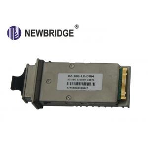
10Gb/s X2 transceiver module NDX2-10G-LR is a hot pluggable in the Z-direction module that is usable in typical router line card applications, Storage, IP network and LAN and compliant to X2 MSA. The NDX2-10G-LR is a fully integrated 10.3Gbit/s optical transceiver module that consists of a 10.3Gbit/s optical transmitter and receiver, XAUI interface, Mux and De-mux with clock and data recovery(CDR).transceiver line uses an uncooled 1310nm DML Laser Diode to achieve 10km over standard single mode fiber as 10GBASE-LR of the IEEE 802.3ae.
Ⅰ.Optical Characteristics
Table 1. Optical Characteristics
| No. |
Parameters |
Symbols |
Min. |
Typ. |
Max. |
Unit |
NOTE |
| 1 |
Center Wavelength |
λC |
1290 |
1310 |
1330 |
nm |
|
| 2 |
Signaling speed |
|
- |
10.3125 |
- |
Gbit/s |
|
| 3 |
Signaling speed variation from nominal |
|
-100 |
- |
+100 |
ppm |
|
| 4 |
Average Optical Power |
Pout |
-5 |
- |
0.5 |
dBm |
|
| 6 |
Side Mode Suppression Ratio |
SMSR |
30 |
- |
- |
dB |
|
| 7 |
Extinction Ratio |
ER |
3.5 |
- |
- |
dB |
|
| 8 |
Off Transmit Power |
Poff |
- |
- |
-30 |
dBm |
|
| 9 |
Receiver Sensitivity |
|
- |
|
-14.4 |
dBm |
|
| 10 |
Receiver Overload |
Rsat |
+0.5 |
- |
- |
dBm |
|
| 11 |
Optical Centre Wavelength |
λC |
1270 |
|
1610 |
nm |
|
| 12 |
Los D-Assert |
ROSd |
|
|
-18 |
dBm |
|
| 13 |
Los Assert |
ROSa |
-32 |
|
|
|
|
| 11 |
Los Hysteresis |
|
0.5 |
- |
- |
dB |
|
Ⅱ.Electrical Performance
Table2. Power Supply Characteristics
| No. |
Parameter |
Symbol |
Min. |
Typ. |
Max. |
Unit |
NOTE |
| 1 |
Supply Voltage |
VCC1 |
3.135 |
3.300 |
3.465 |
V |
|
| 2 |
Supply Voltage |
VCC2 |
1.152 |
1.200 |
1.248 |
V |
|
| 3 |
Supply Current |
ICC1 |
- |
- |
1.0 |
A |
+3.3 V |
| 4 |
Supply Current |
ICC2 |
- |
- |
1.7 |
A |
APS |
| 5 |
Power Consumption |
PDS |
- |
- |
3.5 |
W |
|
| 6 |
Power supply stabilization time |
TDF |
- |
- |
500 |
ms |
|
| 7 |
Initialization Time |
TINIT |
- |
- |
5 |
s |
|
| 8 |
RESET Assert Time |
TRESET |
1 |
- |
- |
ms |
|
| 9 |
Hold Time after rising edge of RESET |
THOLD |
500 |
- |
- |
ms |
|
Table 3. XAUI Driver Characteristics
| No. |
Parameter |
Symbol |
Min. |
Typ. |
Max. |
Unit |
NOTE |
| 1 |
Baud Rate |
|
- |
3.125 |
- |
Gbit/s |
|
| 2 |
Baud Rate Tolerance |
|
-100 |
- |
+100 |
ppm |
|
| 3 |
Differential Amplitude |
|
800 |
- |
1600 |
mVPP |
AC, near-end value |
Table4. 1.2V CMOS Interface Characteristics
| No. |
Parameter |
Symbol |
Min. |
Typ. |
Max. |
Unit |
NOTE |
| 1 |
Input High Voltage |
VIH |
0.84 |
- |
1.5 |
V |
|
| 2 |
Input Low Voltage |
VIL |
-0.3 |
- |
0.36 |
V |
|
| 3 |
Input Pull-down Current |
IIn |
20 |
40 |
120 |
µA |
Vih=1.2V |
| 4 |
Output High Voltage |
VOH |
1.0 |
- |
- |
V |
Pull-up=10k ohm to 1.2V |
| 5 |
Output Low Voltage |
VOL |
- |
- |
0.2 |
V |
| 6 |
Pull up Resistance |
RLASI |
10 |
- |
22 |
k ohm |
|
| 7 |
Capacitance |
CLASI |
- |
- |
10 |
pF |
|
| 8 |
Load Capacitance |
CLoad |
- |
- |
320 |
pF |
|
Table5. MDIO Bidirectional Interface Characteristics
| No. |
Parameter |
Symbol |
Min. |
Typ. |
Max. |
Unit |
NOTE |
| 1 |
Input High Voltage |
VIHM |
0.84 |
- |
1.5 |
V |
|
| 2 |
Input Low Voltage |
VILM |
-0.3 |
- |
0.36 |
V |
|
| 3 |
Output High Voltage |
VOHM |
1.0 |
- |
1.5 |
V |
|
| 4 |
Output Low Voltage |
VOLM |
-0.3 |
- |
0.2 |
V |
|
| 5 |
Pull up Resistance |
RMDIO |
200 |
- |
|
Ohm |
1 |
| 6 |
MDC min high/low time |
THM,TLM |
160 |
- |
- |
ns |
|
| 7 |
MDC Frequency |
1/TCK |
TBD |
- |
2.5 |
MHz |
|
| 8 |
Setup time |
TDIS |
10 |
- |
- |
ns |
|
| 9 |
Hold time |
TDIH |
10 |
- |
- |
ns |
|
| 10 |
MDIO output delay after rising edge of MDC |
TPD |
0 |
- |
300 |
ns |
|
| 12 |
Input Capacitance |
Ci |
- |
- |
10 |
pF |
|
| 13 |
Bus Loading |
CL |
- |
- |
470 |
pF |
|
Note:1 The maximum value of RMDIO depends on bus loading(CL),input capacitance(Ci),and MDC frequency(1/TCK).
Fig 1-X2 Transponder Electrical Pad Layout
Table6. X2 Pin Configuration
| Pin # |
Symbol |
I/O |
Logic |
Description |
| 1 |
GND |
I |
Supply |
Electrical ground |
| 2 |
GND |
I |
Supply |
Electrical ground |
| 3 |
GND |
I |
Supply |
Electrical ground |
| 4 |
RESERVED |
- |
- |
Reserved |
| 5 |
3.3 V |
I |
Supply |
Power |
| 6 |
3.3 V |
I |
Supply |
Power |
| 7 |
APS |
I |
Supply |
Adaptive Power Supply |
| 8 |
APS |
I |
Supply |
Adaptive Power Supply |
| 9 |
LASI |
O |
Open Drain |
Link Alarm Status Interrupt. 10-22k ohm pull up on host. |
| 10 |
RESET |
I |
1.2V CMOS |
TX OFF when MDIO RESET |
| 11 |
VEND SPECIFIC |
- |
- |
Vendor Specific Pin. Leave unconnected. |
| 12 |
TX ON/OFF |
I |
1.2V CMOS |
Transmitter ON/OFF |
| 13 |
RESERVED |
- |
- |
Reserved |
| 14 |
MOD DETECT |
O |
- |
Pulled low inside module through 1k ohm. |
| 15 |
VEND SPECIFIC |
- |
- |
Vendor Specific Pin. Leave unconnected. |
| 16 |
VEND SPECIFIC |
- |
- |
Vendor Specific Pin. Leave unconnected. |
| 17 |
MDIO |
I/O |
Open Drain |
Management Data IO |
| 18 |
MDC |
I |
1.2V CMOS |
Management Data Clock |
| 19 |
PRTAD4 |
I |
1.2V CMOS |
Port Address bit 4 (Low=0) |
| 20 |
PRTAD3 |
I |
1.2V CMOS |
Port Address bit 3 (Low=0) |
| 21 |
PRTAD2 |
I |
1.2V CMOS |
Port Address bit 2 (Low=0) |
| 22 |
PRTAD1 |
I |
1.2V CMOS |
Port Address bit 1 (Low=0) |
| 23 |
PRTAD0 |
I |
1.2V CMOS |
Port Address bit 0 (Low=0) |
| 24 |
VEND SPECIFIC |
- |
- |
Vendor Specific Pin. Leave unconnected. |
| 25 |
APS SET |
O |
- |
Feedback output for APS |
| 26 |
RESERVED |
- |
- |
Reserved for Avalanche Photodiode use. |
| 27 |
APS SENSE |
O |
Analog |
APS Sense Connection |
| 28 |
APS |
I |
Supply |
Adaptive Power Supply |
| 29 |
APS |
I |
Supply |
Adaptive Power Supply |
| 30 |
3.3 V |
I |
Supply |
Power |
| 31 |
3.3 V |
I |
Supply |
Power |
| 32 |
RESERVED |
- |
- |
Reserved |
| 33 |
GND |
I |
Supply |
Electrical Ground |
| 34 |
GND |
I |
Supply |
Electrical Ground |
| 35 |
GND |
I |
Supply |
Electrical Ground |
| 36 |
GND |
I |
Supply |
Electrical Ground |
| 37 |
GND |
I |
Supply |
Electrical Ground |
| 38 |
RESERVED |
- |
- |
Reserved |
| 39 |
RESERVED |
- |
- |
Reserved |
| 40 |
GND |
I |
Supply |
Electrical Ground |
| 41 |
RX LANE 0+ |
O |
AC |
Module XAUI Output Lane 0+ |
| 42 |
RX LANE 0- |
O |
AC |
Module XAUI Output Lane 0- |
| 43 |
GND |
I |
Supply |
Electrical Ground |
| 44 |
RX LANE 1+ |
O |
AC |
Module XAUI Output Lane 1+ |
| 45 |
RX LANE 1- |
O |
AC |
Module XAUI Output Lane 1- |
| 46 |
GND |
I |
Supply |
Electrical Ground |
| 47 |
RX LANE 2+ |
O |
AC |
Module XAUI Output Lane 2+ |
| 48 |
RX LANE 2- |
O |
AC |
Module XAUI Output Lane 2- |
| 49 |
GND |
I |
Supply |
Electrical Ground |
| 50 |
RX LANE 3+ |
O |
AC |
Module XAUI Output Lane 3+ |
| 51 |
RX LANE 3- |
O |
AC |
Module XAUI Output Lane 3- |
| 52 |
GND |
I |
Supply |
Electrical Ground |
| 53 |
GND |
I |
Supply |
Electrical Ground |
| 54 |
GND |
I |
Supply |
Electrical Ground |
| 55 |
TX LANE 0+ |
I |
AC |
Module XAUI Input Lane 0+ |
| 56 |
TX LANE 0- |
I |
AC |
Module XAUI Input Lane 0- |
| 57 |
GND |
I |
Supply |
Electrical Ground |
| 58 |
TX LANE 1+ |
I |
AC |
Module XAUI Input Lane 1+ |
| 59 |
TX LANE 1- |
I |
AC |
Module XAUI Input Lane 1- |
| 60 |
GND |
I |
Supply |
Electrical Ground |
| 61 |
TX LANE 2+ |
I |
AC |
Module XAUI Input Lane 2+ |
| 62 |
TX LANE 2- |
I |
AC |
Module XAUI Input Lane 2- |
| 63 |
GND |
I |
Supply |
Electrical Ground |
| 64 |
TX LANE 3+ |
I |
AC |
Module XAUI Input Lane 3+ |
| 65 |
TX LANE 3- |
I |
AC |
Module XAUI Input Lane 3- |
| 66 |
GND |
I |
Supply |
Electrical Ground |
| 67 |
RESERVED |
- |
- |
Reserved |
| 68 |
RESERVED |
- |
- |
Reserved |
| 69 |
GND |
I |
Supply |
Electrical Ground |
| 70 |
GND |
I |
Supply |
Electrical Ground |
Note: Case is connected to electrical ground in the module.
Ⅴ.Register Definition
| Device Address (Dec) Register Address (Hex) |
PMA/PMD 1 |
PCS 3 |
PHY XS 4 |
| 0x0000 |
PMA/PMD Control1 |
PCS Control1 |
PHY XS Control1 |
| 0x0001 |
PMA/PMD Status1 |
PCS Status1 |
PHY XS Status1 |
| 0x0002 |
PMA/PMD Device Identifier0 |
PCS Device Identifier0 |
PHY XS Device Identifier0 |
| 0x0003 |
PMA/PMD Device Identifier1 |
PCS Device Identifier1 |
PHY XS Device Identifier1 |
| 0x0004 |
PMA/PMD Speed Ability |
PCS Speed Ability |
PHY XS Speed Ability |
| 0x0005 |
PMA/PMD Device in Package1 |
PCS Device in Package1 |
PHY XS Device in Package1 |
| 0x0006 |
PMA/PMD Device in Package2 |
PCS Device in Package2 |
PHY XS Device in Package2 |
| 0x0007 |
10G PMA/PMD Control2 |
PCS Control2 |
Reserved |
| 0x0008 |
10G PMA/PMD Status2 |
PCS Status2 |
PHY XS Status2 |
| 0x0009 |
10G PMD Transmit Disable |
Reserved |
Reserved |
| 0x000A |
10G PMD Receive Signal O.K. |
Reserved |
Reserved |
| 0x000E |
Package Identifier0 |
Reserved |
Reserved |
| 0x000F |
Package Identifier1 |
Reserved |
Reserved |
| 0x0018 |
Reserved |
Reserved |
10G PHY XGXS Lane Status |
| 0x0019 |
Reserved |
Reserved |
10G PHY XGXS Test Control |
| 0x0020 |
Reserved |
10GBASE-R PCS Status1 |
Reserved |
| 0x0021 |
Reserved |
10GBASE-R PCS Status2 |
Reserved |
| 0x0022 |
Reserved |
10GBASE-R PCS Test pattern Seed A0 |
Reserved |
| 0x0023 |
Reserved |
10GBASE-R PCS Test pattern Seed A1 |
Reserved |
| 0x0024 |
Reserved |
10GBASE-R PCS Test pattern Seed A2 |
Reserved |
| 0x0025 |
Reserved |
10GBASE-R PCS Test pattern Seed A3 |
Reserved |
| 0x0026 |
Reserved |
10GBASE-R PCS Test pattern Seed B0 |
Reserved |
| 0x0027 |
Reserved |
10GBASE-R PCS Test pattern Seed B1 |
Reserved |
| 0x0028 |
Reserved |
10GBASE-R PCS Test pattern Seed B2 |
Reserved |
| 0x0029 |
Reserved |
10GBASE-R PCS Test pattern Seed B3 |
Reserved |
| 0x002A |
Reserved |
10GBASE-R PCS Test pattern Control |
Reserved |
| 0x002B |
Reserved |
10GBASE-R PCS Test pattern Error counter |
Reserved |
| 0x8000 |
NVR Control/Status (X2 Register) |
Reserved |
| 0x8007 - 0x807D |
NVR (X2 Register) |
Reserved |
| 0x807E- 0x80AD |
Customer AREA |
Reserved |
| 0x80AE - 0x8106 |
SH Specific Area(X2 Register) |
Reserved |
| 0x9000 |
RX_ALARM Control (X2 Register) |
Reserved |
| 0x9001 |
TX_ALARM Control (X2 Register) |
Reserved |
| 0x9002 |
LASI Control (X2 Register) |
Reserved |
| 0x9003 |
RX_ALARM Status (X2 Register) |
Reserved |
| 0x9004 |
TX_ALARM Status (X2 Register) |
Reserved |
| 0x9005 |
LASI Status (X2 Register) |
Reserved |
| 0x9006 |
TX_FLAG Control Bits |
Reserved |
| 0x9007 |
RX_FLAG Control Bits |
Reserved |
| 0xA000 - 0xA027 |
Alarm and Warning Thresholds |
Reserved |
| 0xA060 - 0xA069 |
Digital Optical Monitoring Interface |
Reserved |
| 0xA06F |
DOM Capability - Extended |
Reserved |
| 0xA070 |
TX_ALARM_FLAG Bits |
Reserved |
| 0xA071 |
RX_ALARM_FLAG Bits |
Reserved |
| 0xA074 |
TX_WARNING_FLAG Bits |
Reserved |
| 0xA075 |
RX_WARNING_FLAG Bits |
Reserved |
| 0xA100 |
Optional Digital Optical Monitoring (DOM) Control/Status |
Reserved |
Ⅵ. Regulatory Compliance
| Feature |
Reference |
Performance |
| Electrostatic discharge(ESD) |
IEC/EN 61000-4-2 |
Compatible with standards |
| Electromagnetic Interference (EMI) |
FCC Part 15 Class B EN 55022 Class B (CISPR 22A) |
Compatible with standards |
| Laser Eye Safety |
FDA 21CFR 1040.10, 1040.11 IEC/EN 60825-1,2 |
Class 1 laser product |
| ROHS |
2002/95/EC |
Compatible with standards |
| EMC |
EN61000-3 |
Compatible with standards |
Appendix A. Document Revision
| Version No. |
Date |
Description |
| 1.0 |
2010-09-01 |
Preliminary datasheet |
| 2.0 |
2011-09-10 |
Update format and company’s logo |