Product Features
● Supports 41.2Gb/s bit rates
● Duplex LC receptacle
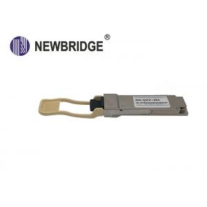
● Hot pluggable QSFP+ form factor
● Uncooled 4x10Gb/s CWDM transmitter
● Applicable for 100m&300m on OM3 MMF,150m&400m on OM4 MMF.
● Built-in digital diagnostic functions
● Low power consumption, < 3.5W
● Unretimed XLPPI electrical interface
● Operating case temperature: -20°C to 75°C
Applications
● 40GBASE-SR4 40G Ethernet
● Datacom/Telecom switch & router connections
● Data Aggregation and Backplane Applications
● Proprietary Protocol and Density Applications
● Infiniband transmission at 4CH SDR, DDR and QDR
● Other optical links
Product Descriptions
The QSFP+ SR is a Four-Channel, Pluggable, Parallel, Fiber-Optic QSFP+ Transceiver for 40 Gigabit Ethernet Applications. This transceiver is a high performance module for short-range multi-lane data communication and interconnect applications. It integrates four data lanes in each direction with 40 Gbps bandwidth.one version is Each lane can operate at 10.5Gbps up to100m using OM3 or 150m using OM4 Multimode fiber,another version is Each lane can operate at 10.5Gbps up to300m using OM3 or 400m using OM4 Multimode fiber These modules are designed to operate over multimode fiber systems using a nominal wavelength of 850nm. The electrical interface uses a 38 contact edge type connector. The optical interface uses an 12 fiber MTP (MPO) connector. This module incorporates proven circuit and VCSEL technology to provide reliable long life, high performance, and consistent service.
Absolute Maximum Ratings
| Parameter | Symbol | Min. | Max. | Unit | Note |
| Supply Voltage | Vcc | -0.5 | 3.6 | V | |
| Storage Temperature | TS | -20 | 85 | °C | |
| Relative Humidity | RH | 0 | 85 | % | |
| Damage Threshold, per Lane | DT | 3.4 | | dBm | |
Note: Stress in excess of the maximum absolute ratings can cause permanent damage to the transceiver.
General Operating Characteristics
| Parameter | Value | Unit | Note |
| Module Form Factor | QSFP+ | | |
| Number of Lanes | 4 Tx and 4 Rx | | |
| Maximum Aggregate Data Rate | 42.0 | Gb/s | |
| Maximum Data Rate per Lane | 10.5 | Gb/s | |
| Protocols Supported | Typical applications include 40G Ethernet, Infiniband, Fibre Channel, SATA/SAS3 | | |
| Electrical Interface and Pin-out | 38-pin edge connector ,Pin-out as defined by the QSFP+ MSA | | |
| Management Interface | Serial, I2C-based, 400 kHz maximum frequency | | |
| Parameter | Symbol | Min | Typ | Max | Units | Note |
| Bit Rate per Lane | BR | 1062 | | 10500 | Mb/sec | 1 |
| Bit Error Ratio | BER | | | 10-12 | | 2 |
| Distance on OM3 MMF (CDS1) | D1 | | | 100 | meters | 3 |
| Distance on OM4 MMF (CDS1) | D2 | | | 150 | meters | 3 |
| Distance on OM3 MMF (CDS3) | D3 | | | 300 | | 4 |
| Distance on OM4 MMF (CDS3) | D4 | | | 400 | | 4 |
Notes:
1. Compliant with 40G Ethernet. Compatible with 1/10 Gigabit Ethernet and 1/2/4/8/10G Fibre Channel.
2. Tested with a PRBS 231-1 test pattern.
3. Per 40GBASE-SR4, IEEE 802.3ba,Belong to part No: OLSQ854XM-CDS1
4. Per 40GBASE-SR4, IEEE 802.3ba,Belong to part No.: OLSQ854XM-CDS3
Optical Characteristics (TOP(C) = 0 to 70 ℃, TOP(I) =-40 to 80 ℃,VCC = 3.13 to 3.47 V)
| Parameter | Symbol | Min. | Typ | Max. | Unit | Note |
| Transmitter |
| Operating Wavelength | λ | 840 | 850 | 860 | nm | |
| Ave. output power (Enabled) | PAVE | -7.5 | | +2.5 | dBm | |
| Difference in launch power between any two lanes (OMA) | DL | | | 4 | dB | |
| Extinction Ratio | ER | 3 | | | dB | |
| Peak power, each lane | PP | | | 4 | dBm | |
| Dispersion penalty, each lane | TDP | | | 3.5 | dB | |
| Average launch power of OFF transmitter, each lane | POFF | | | -30 | dB | |
| Eye Mask coordinates: X1, X2, X3, Y1, Y2, Y3 | SPECIFICATION VALUES 0.23, 0.34, 0.43, 0.27, 0.35, 0.4 | Hit Ratio = 5x10⁻⁵ |
| Receiver |
| Operating Wavelength | λc | 840 | 850 | 860 | nm | |
| Stressed receiver sensitivity in OMA(OLSQ854XM-CDS1) | PSEN1 | | | -5.4 | dBm | 3 |
| Stressed receiver sensitivity in OMA(OLSQ854XM-CDS3) | PSEN2 | | | -7.5 | dBm | 3 |
| Average Receive Power,each lane | PAVE | -11 | | +2.4 | dBm | |
| Receiver Reflectance | Rrx | | | -12 | dB | |
| LOS Assert | Pa | -30 | | | dBm | |
| LOS De-assert | Pd | | | -9 | dBm | |
| LOS Hysteresis | Pd-Pa | 0.5 | | | dB | |
Notes:
Measured with conformance test signal at TP3 for BER = 10e-12 Receiver Characteristics
Top side Bottom side
| Pin | Symbol | Name/Description | Notes |
| 1 | GND | Ground | 1 |
| 2 | Tx2n | Transmitter Inverted Data Input | |
| 3 | Tx2p | Transmitter Non-Inverted Data Input | |
| 4 | GND | Ground | 1 |
| 5 | Tx4n | Transmitter Inverted Data Input | |
| 6 | Tx4p | Transmitter Non-Inverted Data Input | |
| 7 | GND | Ground | 1 |
| 8 | ModSelL | Module Select | 1 |
| 9 | ResetL | Module Reset | |
| 10 | Vcc Rx | +3.3 V Power supply receiver | |
| 11 | SCL | 2-wire serial interface clock | |
| 12 | SDA | 2-wire serial interface data | |
| 13 | GND | Ground | 1 |
| 14 | Rx3p | Receiver Non-Inverted Data Output | |
| 15 | Rx3n | Receiver Inverted Data Output | |
| 16 | GND | Ground | 1 |
| 17 | Rx1p | Receiver Non-Inverted Data Output | |
| 18 | Rx1n | Receiver Inverted Data Output | |
| 19 | GND | Ground | 1 |
| 20 | GND | Ground | 1 |
| 21 | Rx2n | Receiver Inverted Data Output | |
| 22 | Rx2p | Receiver | Non-Inverted |
| 22 | Rx2p | Receiver Non-Inverted Data Output | |
| 23 | GND | Ground | 1 |
| 24 | Rx4n | Receiver Inverted Data Output | |
| 25 | Rx4p | Receiver Non-Inverted Data Output | |
| 26 | GND | Ground | 1 |
| 27 | ModPrsL | Module Present | |
| 28 | IntL | Interrupt | |
| 29 | Vcc Tx | +3.3 V Power supply transmitter | |
| 30 | Vcc1 | +3.3 V Power Supply | |
| 31 | LPMode | Low Power Mode | |
| 32 | GND | Ground | 1 |
| 33 | Tx3p | Transmitter Non-Inverted Data Input | |
| 34 | Tx3n | Transmitter Inverted Data Input | |
| 35 | GND | Ground | 1 |
| 36 | Tx1p | Transmitter Non-Inverted Data Input | |
| 37 | Tx1n | Transmitter Inverted Data Input | |
| 38 | GND | Ground | 1 |
Power Supply Filtering

Package Dimensions
Ordering Information
| Part Number | Description |
| QSFP-40G-SR4-CDS1 | QSFP+,40Gb/s, 850nm, 100m, -20~75℃ MPO |
| QSFP-40G-SR4-CDS3 | QSFP+,40Gb/s, 850nm, 300m, -20~75℃ MPO |